 Mila
Apr 13,2026
100
Mila
Apr 13,2026
100
Why 90% of EMC Issues Come from Poor Grounding in PCB Design
During hardware development, failing EMC tests is a common issue. Many engineers try fixes such as adding shielding enclosures, replacing chips, or increasing capacitance. However, these approaches of...
Mila
Apr 10,2026
293
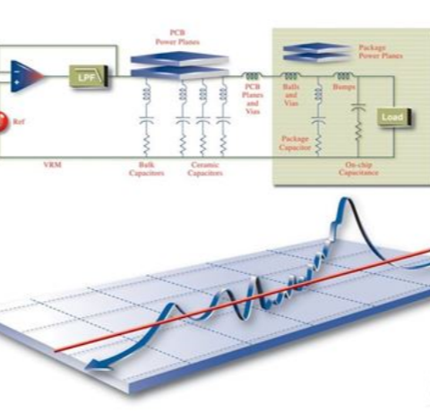
PDN Design Guidelines for HDI PCB: Key Optimization Techniques for Stable Power Delivery
PDN (Power Distribution Network) is a critical part of PCB design, directly determining power delivery efficiency, noise suppression capability, and overall system stability. Skipping PDN simulation a...
Mila
Apr 09,2026
524
PMU PCB Design Guidelines: Layout and Routing Best Practices for Power Management
The PMU (Power Management Unit) is the core of power supply systems in electronic devices such as smartphones and computers. It is responsible for voltage and current regulation, power switching, batt...
Mila
Apr 07,2026
387
Mixed Signal PCB Design: Common Interference Issues and Practical Solutions
In electronic design, interference in mixed-signal systems is a common challenge for engineers. Digital circuits have strong noise immunity, while analog circuits are highly sensitive—even minor inter...
Mila
Apr 03,2026
449
Why Should Power Planes Be Smaller Than Ground Planes in PCB Design?
In multilayer PCB design, there is a widely accepted guideline: power planes should be slightly smaller than ground planes, with a uniform edge inset instead of matching the board outline.Many enginee...
Mila
Mar 31,2026
723
PCIe PCB Layout Guidelines: Key Design Rules for High-Speed Routing
What is PCI Express (PCIe)PCI Express (PCIe) is a high-speed serial computer expansion bus standard. It adopts a point-to-point, dual-channel architecture that provides dedicated bandwidth for each co...
Mila
Mar 26,2026
625
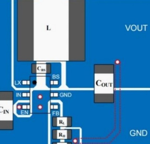
LDO Power PCB Layout Design Guidelines: From Basics to Best Practices
In power supply design, linear regulators (LDOs) are widely used in portable devices, industrial control systems, and consumer electronics due to their simple circuitry, low ripple, and fast transient...
Mila
Mar 24,2026
802
Jumper Wires in PCB Design: Functions, Applications, and Best Practices
In PCB design, multilayer boards, with their sophisticated stack-up structures and complex via technologies, make it possible to achieve highly flexible and nearly “limitless” routing. However, in cos...
Mila
Mar 20,2026
676
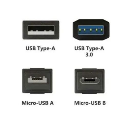
USB 2.0 vs USB 3.0 vs USB4 PCB Layout Differences
Since the USB Implementers Forum released the USB 1.0 standard in 1996, USB technology has evolved through multiple generations, including USB 1.1, USB 2.0, USB 3.0, USB 3.1, and USB 3.2. In 2019, the...
Mila
Mar 17,2026
648
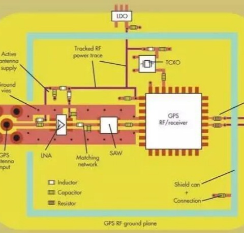
Top 10 RF PCB Layout Mistakes and How to Avoid Them
RF PCB layout is a critical step that determines the actual performance of a circuit, directly affecting impedance matching, signal integrity, EMC performance, and long-term stability. In the previous...
Mila
Mar 06,2026
387
Embedded Components in High Current PCB Layout: Advantages and Implementation Methods
Key Advantages of Embedded Components in High Current PCB LayoutEnhanced Current Carrying CapabilityBy embedding copper blocks, copper bars, or high-power shunt resistors inside the PCB, the effective...
Mila
Mar 05,2026
920
Thermal Resistance and Heat Flow in LED PCB Design: Understanding LED PCB Layout for Better Heat Dissipation
In the previous LED PCB Layout article, we discussed several practical considerations for LED PCB layout and routing. Proper placement and routing are essential for achieving reliable LED performance....
Mila
Feb 27,2026
1823
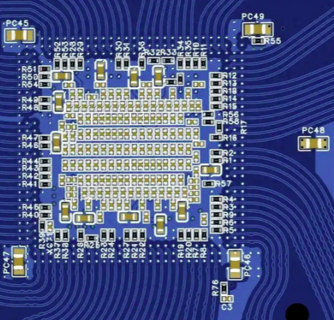
PCB Layout Best Practices for Improved Performance and Manufacturability
During the PCB design process, component placement plays a critical role. A well-planned and scientific layout not only makes the board look clean and organized, but also effectively controls trace le...
Mila
Feb 25,2026
1290
DDR2 PCB Layout Guidelines: Routing, Termination, and Design Principles
In modern high-speed digital circuit design, DDR2 memory remains a widely used high-speed storage device. Due to its high operating frequency, the quality of the DDR2 PCB layout directly determines wh...
 William Harter
Feb 13,2026
562
William Harter
Feb 13,2026
562
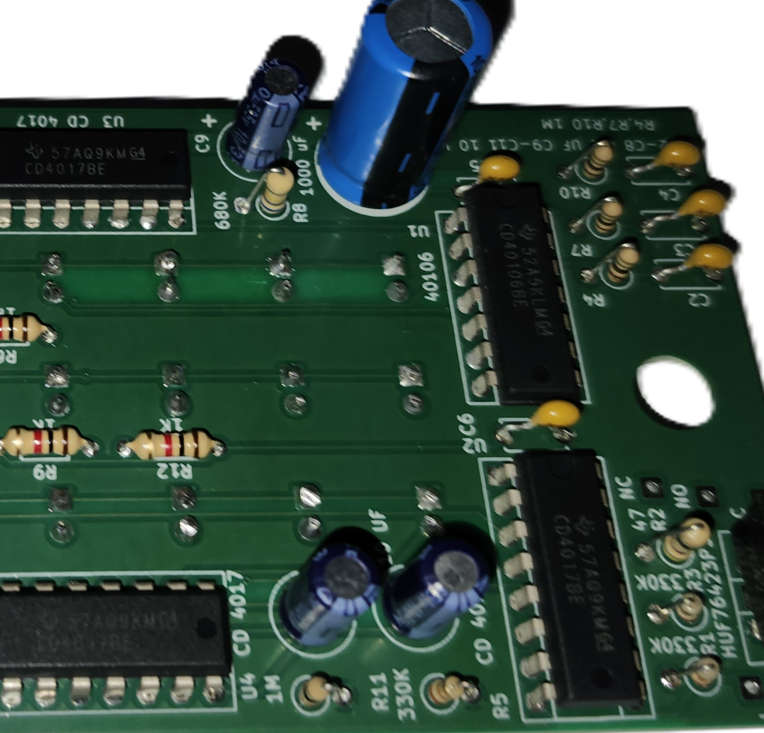
Using Inspection Tools When Designing PC Boards
When designing PC boards in KiCad (or similar software), always use the Electrical Rules Checker for schematics and the Design Rules Checker for board layouts. Run the Electrical Rules Checker before ...
Mila
Feb 09,2026
948
Inverter PCB Layout Guidelines: Best Practices for High-Efficiency and Low-EMI Power Design
As one of the core components of an inverter, the transformer directly affects the overall system efficiency and reliability. In PCB layout design, the transformer’s placement, surrounding environment...
Mila
Jan 30,2026
2059
DDR3 PCB Layout and Routing Guide: Topology, Placement, and Signal Integrity Tips
DDR3 layout and routing are highly demanding, requiring careful attention to signal integrity, timing, and design constraints. The following summarizes the key design process, component placement stra...
Mila
Jan 29,2026
1429
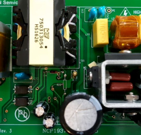
AC-DC PCB Layout Guidelines: Safety, Isolation, and EMI Control
In intelligent switched-mode power supply design, the current-loop layout of an AC-DC converter is critical to the overall system performance. A well-designed layout can improve power efficiency, redu...
Mila
Jan 28,2026
1653
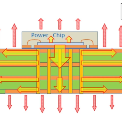
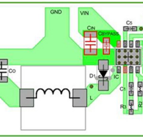
DC-DC Converter PCB Layout Guidelines: Power Loops, Hot Loops, and EMI Control
The quality of a DC-DC converter design is determined not only by the chosen topology and component parameters, but very often by the PCB layout, which can ultimately decide the success or failure of ...
Mila
Jan 23,2026
1232
PCB Component Placement Guidelines: A Practical Layout Strategy
Functional Zoning Comes FirstDuring the PCB layout stage, functional zoning should always be performed before placing any components. Jumping directly into component placement often leads to higher co...
| Ranking | Name | Answers |
|---|---|---|
| 1 | PCBWay Team | 3 |
| 2 | LouD _ | 2 |
| 3 | Dave | 1 |


